1. Running TARA on Basys 3
The Basys 3 is small enough for a student lab bench, inexpensive compared with larger FPGA development boards, and still has exactly the I/O TARA needs to feel like a real computer rather than a hidden simulation: slide switches for mode control, pushbuttons for stepping and input, LEDs for fast visual feedback, a four-digit seven-segment display for register inspection, VGA for graphics, a USB keyboard port for games, and a USB-UART link back to the computer.
That combination makes the board a useful bridge between simulation and physical hardware. You can load a program with TARA Studio, run the same machine code on the FPGA without resynthesizing the hardware, pause the live CPU, read registers directly on the board, inspect memory from TARA Studio, and watch pixels appear on a VGA monitor. The important habit is to treat the board and the monitor as two views of the same machine.
What the board gives you
The board controls are not decorative: SW0 pauses and runs the
CPU, BTNU single-steps it, the seven-segment display can show
PC/IR/registers, and the LEDs expose halt, flags, T-state, and debug bits.
What TARA Studio gives you
The FPGA Tool is the software control desk: program the FPGA itself
after a cold boot, connect over USB, load a .tara program,
inspect live memory, and pause the board before deliberate memory edits.
T0, fetch at
T1, decode at T2, execute at T3. Loads and
pops take more.
2. Board Orientation
Use the labeled board photo as your first map. The numbered callouts are the standard Digilent Basys 3 references, but the table below translates them into TARA CPU roles. Once those roles are familiar, most lab work becomes a loop of setting switches, pressing a button, reading the LEDs or seven-segment display, and deciding what to inspect next.
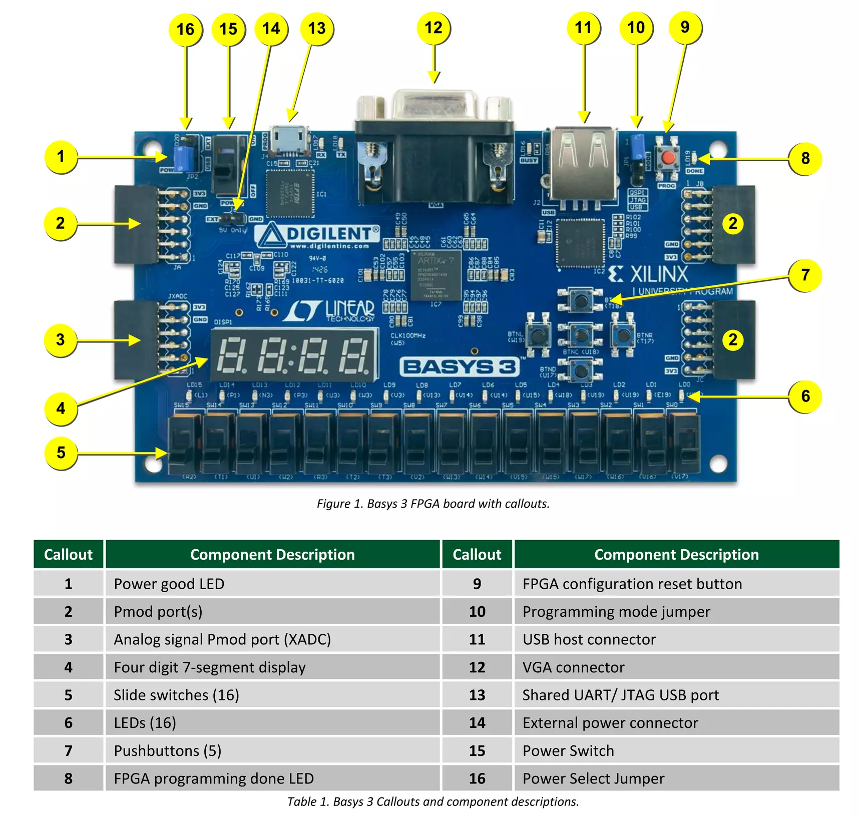
SW0 and LD0
are at the right end of the switch/LED row, while SW15 and
LD15 are at the left end. The five pushbuttons are labeled by
position: center is BTNC, top is BTNU, bottom is
BTND, left is BTNL, and right is BTNR.
| Photo callout | Board part | TARA use |
|---|---|---|
| 4 | Four-digit seven-segment display | Shows one selected 16-bit value in hex: PC, IR, a selected register, or raw switches. |
| 5 | 16 slide switches | Run/pause, speed, optional loader enable, quit key, 7-seg source, and register select. |
| 6 | 16 LEDs | Live CPU dashboard: halted, loading, flags, T-state, and low bits of R0. |
| 7 | Five pushbuttons | btnC resets; btnU single-steps and also means UP; btnD/L/R are game directions. |
| 8 | FPGA DONE LED | Lights when the Artix-7 fabric has successfully loaded a bitstream. |
| 9 | Red PROG button | Clears the FPGA configuration and reloads it from the source selected by JP1. This is not the TARA CPU reset button. |
| 10 | JP1 programming-mode jumper | Use QSPI/SPI to boot the persistent flash image. JTAG programming still works while the jumper is in either position. |
| 11 | USB host connector | Keyboard input for games: arrows or WASD. The Q key requests reset. |
| 12 | VGA connector | Shows the 64x64 framebuffer scaled to 640x480 with a banner and reset splash. |
| 13 | Shared UART/JTAG micro-USB | Programs the FPGA and carries the serial memory link used by TARA Studio. |
| 15 | Power switch | Turns the board on after the USB cable or external supply is connected. |
| 16 | Power select jumper | For normal lab use, select USB power when powering from the programming cable. |
| 2, left JA Pmod | Pmod JA header | Optional ESP32 serial loader: JA[0]=sdata, JA[1]=sclk, JA[2]=active. |
3. Program the FPGA
Programming the Basys 3 means loading the synthesized TARA hardware into
the FPGA. This is different from loading a TARA assembly program: the
bitstream defines the processor, memory system, VGA path, USB memory link,
and board controls, while a .tara program is ordinary data
that the processor later fetches from memory. If you use TARA Studio,
changing an assembly program usually does not require this step. Rebuild
the bitstream only when the Verilog, course-provided boot image,
constraints, or hardware configuration change.
tara_top.bit) creates the TARA CPU and its peripherals.
A TARA assembly file (something.tara) is a program that runs
on that CPU. Configure the hardware occasionally; load .tara
programs as often as you like without rebuilding the bitstream.
Physical setup
- Set the power-select jumper at callout 16 to USB power, unless you are intentionally using an external supply.
- Connect a known data-capable micro-USB cable at callout 13. This one cable carries both JTAG programming and the UART memory link.
- Turn on the power switch at callout 15 and confirm the power-good LED at callout 1.
- For persistent boot, place the JP1 mode jumper at callout 10 in the position marked QSPI. Turn the board off before moving the jumper.
- Optional: attach VGA at callout 12 and a USB keyboard at callout 11.
Choose the result you need
| Method | What changes | Survives power-off? | Best use |
|---|---|---|---|
| FPGA SRAM via JTAG | Configures the FPGA immediately in a few seconds. | No | Normal development, labs, and the fastest first-success test. |
| SPI/QSPI flash via JTAG | Writes the non-volatile flash; the FPGA loads it on the next configuration cycle. | Yes, when JP1 is at QSPI | Standalone demos and boards that should start TARA after every power cycle. |
| Vivado build + JTAG | Rebuilds tara_top.bit from RTL, then configures the attached board. |
No, unless you later write that bitstream to flash | Hardware developers changing Verilog, constraints, or initialization files. |
A. Program an existing bitstream from TARA Studio
- Open the TARA FPGA Tool tab.
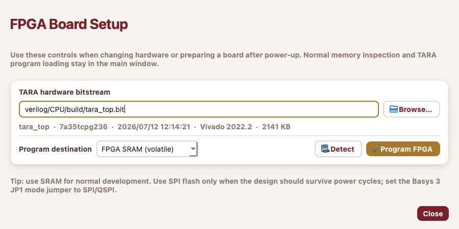
- Choose Board Setup from the menu at the top.
- Browse to
verilog/CPU/build/tara_top.bit, or to the bitstream supplied for your lab. - Read the summary beneath the path. The TARA design should be
tara_topand the Basys 3 device should begin with7a35t(normally7a35tcpg236). - Press Detect if you want a non-destructive cable and JTAG-chain check.
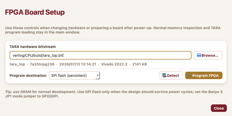
- Select FPGA SRAM (volatile) or SPI flash (persistent), then press Program FPGA.
Recommended first test: SRAM/JTAG
- Leave the board powered and connected by USB.
- Select FPGA SRAM (volatile) and press Program FPGA.
- Wait for the success message and confirm that the DONE LED at callout 8 is on.
- Open Connect Memory and connect to FPGA USB as described in section 5.
SRAM programming is deliberately temporary. A cold power cycle clears the FPGA, so repeat these four steps unless you have installed a flash image. After a successful SRAM load, TARA Studio rescans the serial ports and attempts to reconnect if FPGA USB was already selected.
Install and boot a persistent SPI/QSPI image
- Turn the Basys 3 off, move JP1 at callout 10 to QSPI, and turn it back on.
- In Board Setup, select SPI flash (persistent) and press Program FPGA.
- Accept the confirmation and leave the board powered while the flash is erased and written. This takes longer than SRAM programming.
- When TARA Studio reports that flash was written, press the red PROG button at callout 9 or power-cycle the board.
- Confirm the DONE LED at callout 8 lights and, if attached, the VGA display shows the TARA splash.
- Connect memory. A later power cycle should repeat steps 4–5 automatically because JP1 remains at QSPI.
Command-line equivalents
TARA Studio uses openFPGALoader. The same operations are available from a shell:
# Check that JTAG can see the board; does not program anything
openFPGALoader -b basys3 --detect

# Configure FPGA SRAM now; erased by power-off
openFPGALoader -b basys3 verilog/CPU/build/tara_top.bit

# Write the persistent SPI/QSPI flash image
openFPGALoader -b basys3 -f verilog/CPU/build/tara_top.bitbrew install openfpgaloader. On Linux, install it from your
package manager or from source and install the project's udev rules so
the board is reachable without sudo. If the binary is in an
unusual location, the setup prompt lets you locate it.
B. Build and program from the CPU directory
cd verilog/CPU
vivado -mode batch -source hardware/build.tcl
The script gathers the RTL, applies tara_basys3.xdc, points Vivado at
the required memory initialization files, writes build/tara_top.bit, and programs the
attached board when hardware is available.
Build only
vivado -mode batch -source hardware/build.tcl -tclargs noprogramUse this when you want reports and a bitstream but do not want to touch the connected board.
Hand the bitstream on
build/tara_top.bit is self-contained. Copy it to any machine with
TARA Studio and route A will program a board from it, so only one person in a
lab needs Vivado installed.
After programming
- The FPGA configuration done LED near callout 8 should indicate that programming completed.
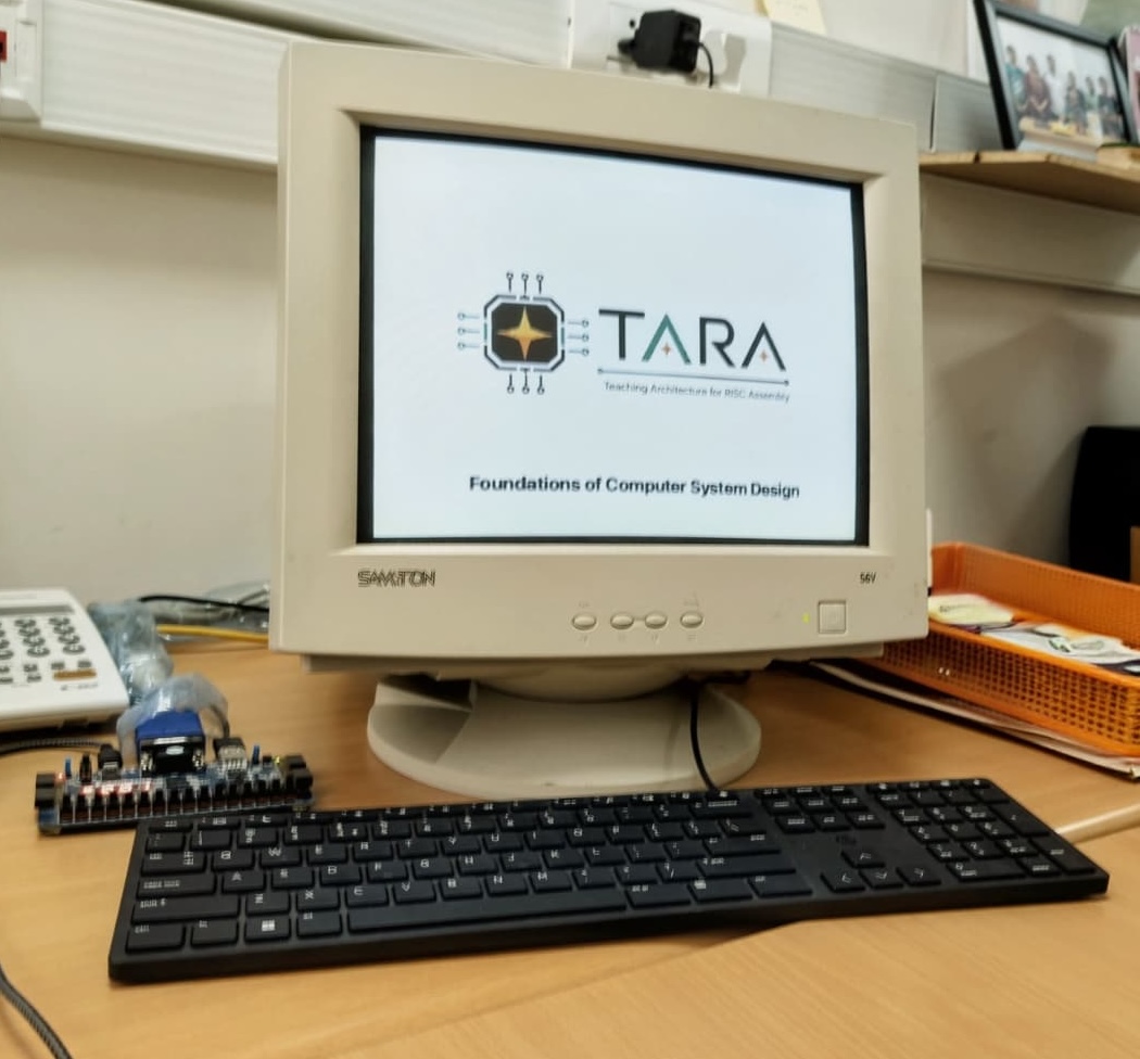
- On a VGA monitor, reset or power-up shows the TARA splash for about two seconds.
- During the splash, the CPU is held at reset, so a fast program cannot run to completion behind the splash.
- After the splash, the CPU starts from
PC=0x000unless held by TARA Studio during a program load, the loader, or reset.
4. Runtime Controls
The slide switches, buttons, seven-segment display, and LEDs are wired as a compact hardware debugger. These are live FPGA signals, so they keep working even when TARA Studio is not connected. In single-step mode, the board becomes especially useful because each press advances the machine by one micro-state and the LEDs show which part of the fetch/decode/execute sequence you are looking at.
Switches
| Switch | Meaning | Use during debugging |
|---|---|---|
sw[0] | 1 = auto-run, 0 = single-step mode | Flip down to pause at the next stable step-clock level; flip up to run. |
sw[1] | Auto-clock speed when sw[0]=1: 1 fast, 0 slow | Use slow to watch LEDs; use fast for games and full-speed demos. |
sw[2] | Optional ESP32 loader enable | Leave at 0 for normal use. Set 1 only when an ESP32 is actually driving JA. |
sw[4] | Game QUIT input bit | Appears as bit 4 when a program reads byte 0x5FF. |
sw[13:11] | Register number for the seven-segment display | When register display is selected, choose 000=R0 through 111=R7. |
sw[15:14] | Seven-segment source | 00=PC, 01=IR, 10=selected register, 11=raw switches. |
Buttons
| Button | TARA function | Notes |
|---|---|---|
btnC | Reset | Stretches reset for about 10 ms, restarts the splash, clears halted state, and restarts from PC 0 after release. |
btnU | Single-step clock in pause mode; UP game input | In sw[0]=0, one press advances one CPU micro-state. In games, it also sets bit 0 of 0x5FF. |
btnD | DOWN game input | Sets bit 1 of 0x5FF. |
btnL | LEFT game input | Sets bit 2 of 0x5FF. |
btnR | RIGHT game input | Sets bit 3 of 0x5FF. |
Seven-segment display
The four digits show one 16-bit value in hexadecimal. Set sw[15:14]
first, then use sw[13:11] if you selected a register.
Read PC
Set sw[15:14]=00. This is the next byte address the CPU is fetching or about to fetch.
Read IR
Set sw[15:14]=01. This shows the current instruction word after fetch/decode.
Read a register
Set sw[15:14]=10, then select R0..R7 with sw[13:11].
LED dashboard
| LED bits | Signal | What to watch |
|---|---|---|
led[15] | halted | Turns on after HLT. Reset clears it. |
led[14] | loading | On while the optional JA loader is active. TARA Studio can also hold reset briefly while loading a program over USB. |
led[13:10] | Z,N,C,V | Status bits latched by arithmetic/logic instructions. Branches do not use these flags; they test registers directly. |
led[9:8] | Reserved zeros | Always off in this implementation. |
led[7:5] | Tstate[2:0] | Shows the current micro-state T0..T7. This is the best visual cue while single-stepping. |
led[4:0] | R0[4:0] | Low five bits of R0, useful for simple counters or input/debug programs. |
5. TARA Studio FPGA Tool
The TARA FPGA Tool is organized around how often a control
is needed. One-time hardware work lives under Board Setup,
target selection lives under Connect Memory, and the main
workspace stays focused on reading, changing, and visualizing memory. The
program row remains at the bottom because choosing and running
.tara files is a normal part of every session.
Board Setup
Detect JTAG, inspect a .bit header, and program FPGA SRAM or persistent SPI flash.
Connect Memory
Choose physical FPGA USB or the local simulator, then establish the memory connection.
Main workspace
Read, poll, edit, and visualize memory; browse to a program and load it.
Connect to FPGA memory
- Confirm the DONE LED is on. If it is off, return to Board Setup in section 3.
- Choose Connect Memory from the top menu.
- Select FPGA USB and press Rescan.
- Choose the Basys 3 UART serial endpoint, then press Connect.
- Wait for a green connected: message. You may close the dialog; the connection remains active.
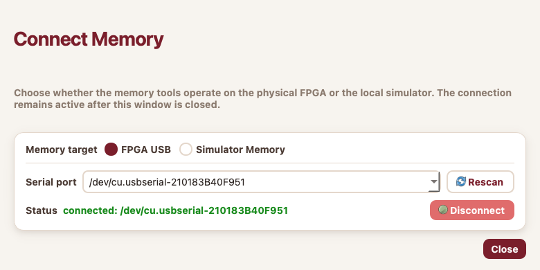
When two Digilent ports appear
The Basys 3 USB interface exposes separate JTAG and UART channels.
TARA Studio ranks the likely UART channel first and remembers the last
port that answered successfully. On the board used for this manual,
macOS presented names ending in ...950 and
...951; ...951 was the UART.
Do not memorize that exact name. If Connect reports no response, try the other Digilent endpoint after confirming that DONE is on and the TARA bitstream is current.
pyserial. Install
it in that same environment with python -m pip install pyserial,
restart TARA Studio, and rescan.
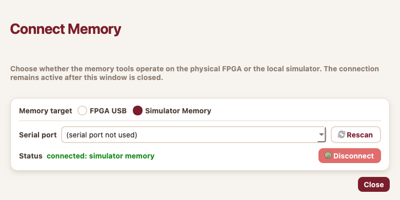
Connect to simulator memory
Choose Connect Memory → Simulator Memory → Connect when you want the same memory workflow without hardware. Serial-port controls are disabled because no USB port is used. Switching targets disconnects the old target first, which prevents an edit intended for the simulator from reaching the FPGA or vice versa.
Load and run a TARA program
- Connect the desired memory target.
- At the bottom of the main window, press Browse and choose a
.tarasource file. - For deliberate hardware single-stepping, set
SW0=0before loading. - Press Load & Run. TARA Studio assembles the source, holds the target while writing its instruction words at
0x000, and then releases it. - On hardware, set
SW0=1for continuous execution or leave it at 0 and useBTNUto advance micro-states.
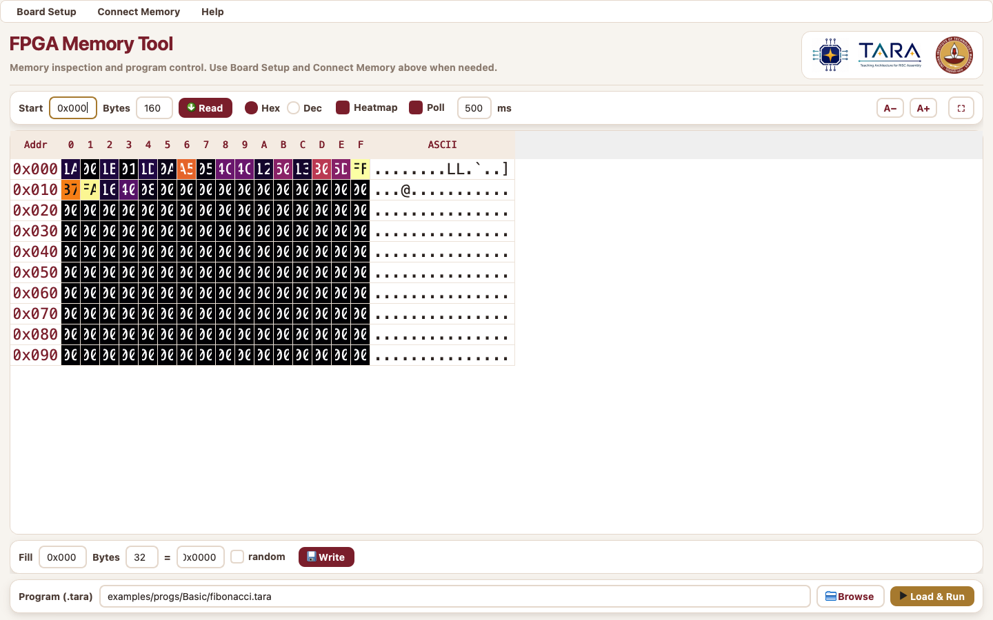
0x000, but it does
not reset the memory viewer's Start field. If you
were watching data at 0x100 or the framebuffer at
0x600, that view remains selected until you change it manually.
Read and understand memory
| Control | What it does | Useful habit |
|---|---|---|
| Start + Bytes | Selects the byte-addressed range to show. Reads are word-based, so an odd Start is aligned to the preceding even address. | Use 0x000 for code, your program's data address for variables, or 0x600 for pixels. |
| Read | Fetches the selected range immediately. | Turn Poll off when you want a stable snapshot. |
| Hex / Dec | Changes only how each byte is displayed. | Hex matches addresses and machine code; decimal is convenient for numeric arrays. |
| Heatmap | Colors bytes by value so patterns and changing regions stand out. | Disable it when changed-byte and framebuffer-region tints are more useful. |
| Poll + interval | Continuously re-reads the selected range. | Start near 500 ms; very fast polling competes with the running CPU for memory access. |
| A− / A+ | Changes the grid font and byte-cell width. | Use A+ before projection or demonstrations. |
| Full screen | Moves the read toolbar, grid, and write toolbar into a full-screen window. | The 16 byte columns stretch across the available width; press Esc to return. |
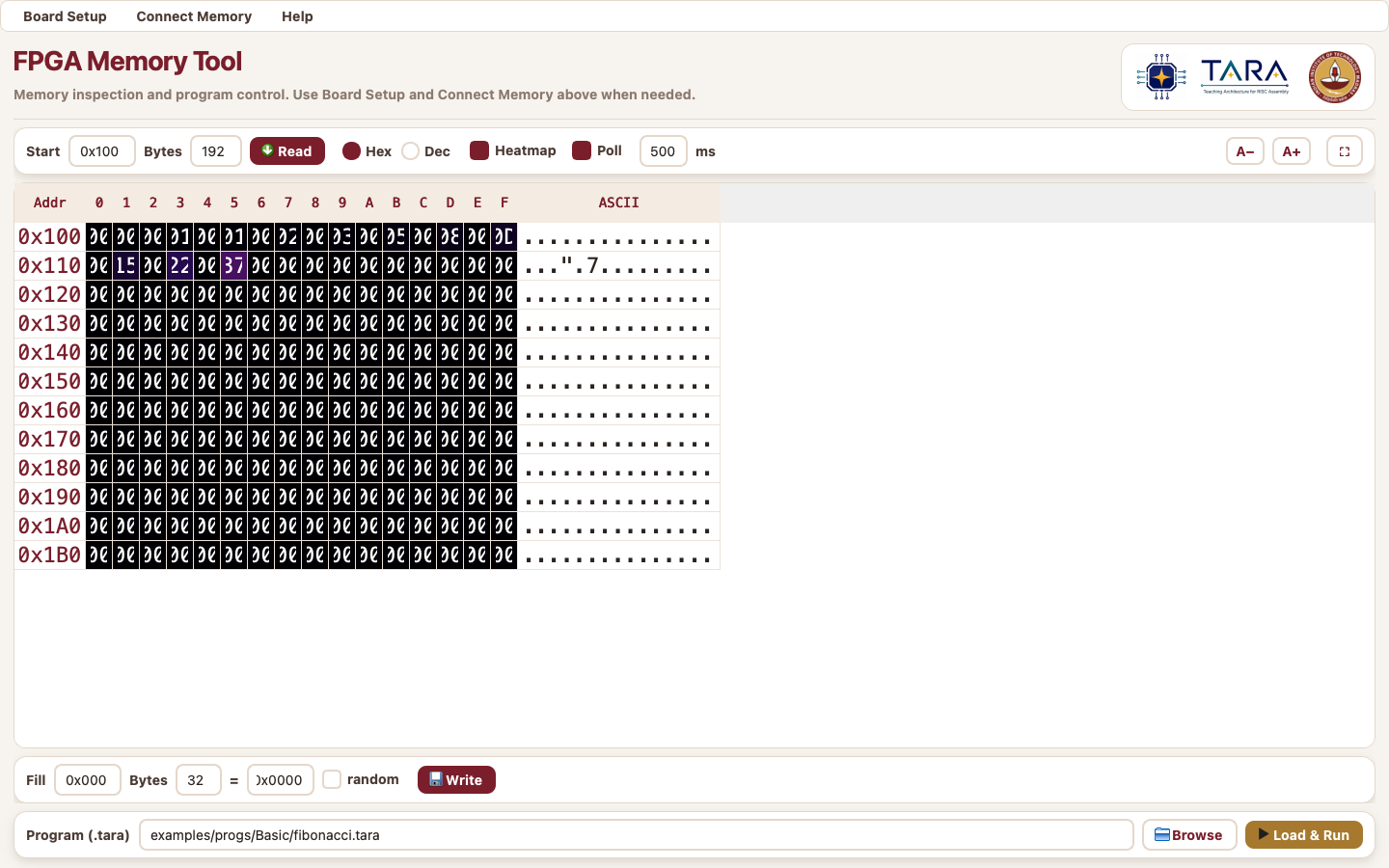
0x100. The viewer remains here even
after another program is loaded at 0x000.
Address patterns worth knowing
0x000: first instruction and normal load address.0x000–0x5FE: ordinary program, data, and stack space.0x5FF: live button/keyboard/quit input byte.0x600–0x7FF: 512-byte framebuffer consumed by VGA.
The UART protocol transfers 16-bit words in big-endian byte order.
For example, word 0x1A00 appears as bytes
1A 00 in adjacent grid cells.
Write and poke memory safely
- Pause a physical TARA CPU with
SW0=0before changing memory that its program may also write. - To change one byte, double-click its grid cell, enter a two-digit hexadecimal value, and accept.
- To initialize a region, use Fill, Bytes, and the 16-bit value beside the equals sign, then press Write.
- Select random when testing display or memory patterns instead of repeating one word.
- Read the range again and confirm the intended bytes changed.
Inspect the framebuffer comfortably
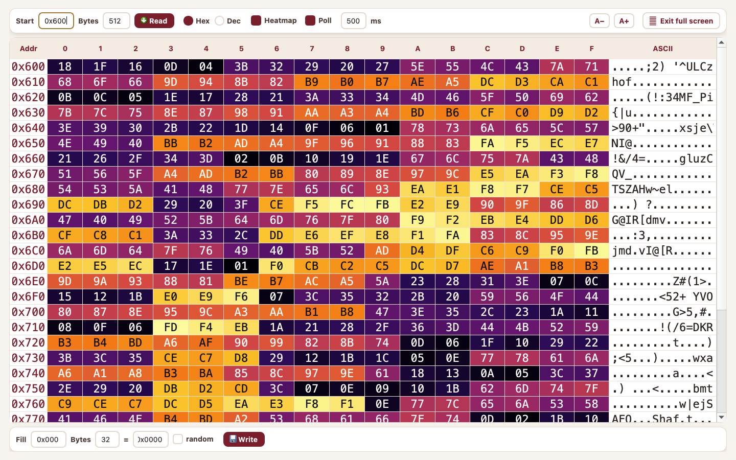
Set Start to 0x600, Bytes to
512, enable Heatmap, and enter full screen. Each row contains
sixteen consecutive bytes, so the entire framebuffer is 32 memory rows.
Full-screen mode stretches every byte cell horizontally to prevent values
from overlapping on a wide display.
Watch the complete array workflow
This 48-second recording uses a physical Basys 3. It programs and verifies
tara_top.bit in SPI flash, connects the FPGA USB memory UART,
reads 256 bytes at 0x400, enlarges the grid with A+ four times,
writes random bytes, runs Bubble Sort in full screen, then runs Reverse
Array on the same hardware memory.
0x400–0x4FF. The
recording uses decimal cells, Heatmap, full screen, enlarged fonts,
and byte-for-byte result verification.
sw[15:14], sw[13:11], btnU, and the
LEDs to inspect execution.
6. Fibonacci Walkthrough
This example computes F(10)=55 and leaves the answer in
R6=0x0037. It is a good runtime-debugging program because it uses
immediate loads, arithmetic, a branch, a jump, a loop counter, and HLT.
; Iterative Fibonacci: F(10) = 55
; R2 = a, R3 = b, R4 = a+b, R5 = counter, R6 = result

        LIL  R2, 0
        LIL  R3, 1
        LIL  R5, 10

loop:   BZ   R5, done
        ADD  R4, R2, R3
        MOV  R2, R3
        MOV  R3, R4
        ADDI R5, -1
        JMP  loop

done:   MOV  R6, R2
        HLT
Load it
- Open TARA Studio, select the TARA FPGA Tool, and connect to the board as described in Section 5.
- Use Browse to select
python-sim/tara_simulator_fpga/src/examples/progs/Basic/fibonacci.tara, or paste the program above into your own.tarafile. - Set
sw[0]=0before clicking Load & Run. TARA Studio releases the CPU, but with run disabled the CPU will wait for button-driven steps. - Set
sw[15:14]=00to watch PC first.
Expected assembled words
| Address | Word | Instruction | Why it matters |
|---|---|---|---|
0x000 | 0x1A00 | LIL R2, 0 | Set a=0. |
0x002 | 0x1B01 | LIL R3, 1 | Set b=1. |
0x004 | 0x1D0A | LIL R5, 10 | Loop count. |
0x006 | 0xA505 | BZ R5, done | Exit when the counter reaches zero. |
0x008 | 0x4C4C | ADD R4, R2, R3 | Compute next Fibonacci value. |
0x00A | 0x1260 | MOV R2, R3 | Advance a. |
0x00C | 0x1380 | MOV R3, R4 | Advance b. |
0x00E | 0x5DFF | ADDI R5, -1 | Count down. |
0x010 | 0xB7FA | JMP loop | Repeat from 0x006. |
0x012 | 0x1640 | MOV R6, R2 | Copy result to R6. |
0x014 | 0x0800 | HLT | Stop the CPU and light led[15]. |
Single-step from reset
- Press
btnC. Wait for the splash to finish. Keepsw[0]=0. - Set
sw[15:14]=00. The seven-segment display should start at or near0000. - Press
btnUrepeatedly. Watchled[7:5]move through T-states. - After the first instruction completes, PC has advanced to
0002. SinceLIL R2,0writes zero, the register value may not visibly change. - Set
sw[15:14]=10andsw[13:11]=011to viewR3. Step until the second instruction completes; the display should read0001. - Set
sw[13:11]=101to viewR5. Step until the third instruction completes; the display should read000A. - Leave the board in single-step mode and continue stepping through the loop.
R5counts down, whileR2andR3walk through Fibonacci values. - When
R5=0000, the nextBZbranches to0x012. Switch the seven-segment display to PC if you want to see that branch land. - Select
R6withsw[13:11]=110. AfterMOV R6,R2, the display reads0037. - After the final
HLT,led[15]turns on. The CPU is halted until reset.
Run, pause, inspect, resume
- Reset with
btnC, then setsw[0]=1andsw[1]=0for slow auto-run. - Watch the T-state LEDs move quickly and the PC/register display update.
- Flip
sw[0]=0to pause into single-step mode. - Use
sw[15:14]andsw[13:11]to inspect PC, IR, R2, R3, R5, and R6. - Press
btnUfor one micro-state at a time, or flipsw[0]=1to resume auto-run.
Final expected state
| Register | Expected value | Meaning |
|---|---|---|
R2 | 0x0037 | F(10) |
R3 | 0x0059 | F(11) |
R4 | 0x0059 | Last computed temporary. |
R5 | 0x0000 | Counter exhausted. |
R6 | 0x0037 | Published answer. |
PC | 0x0016 | HLT was fetched from 0x014, then PC advanced by 2. |
7. VGA, Keyboard, Games
The unified memory exposes both input and display as ordinary addresses from the program's point of view. That is the key simplification: a game does not call a graphics library or an input driver. It reads one byte to learn which buttons are pressed, and it writes bytes into the framebuffer to draw pixels.
Input port 0x5FF
A byte read from 0x5FF returns
{3'b000, QUIT, RIGHT, LEFT, DOWN, UP}.
Buttons and keyboard bits are ORed together before the CPU sees them.
Q requests reset like btnC.
Framebuffer 0x600-0x7FF
The VGA scaler continuously reads 512 framebuffer bytes and displays a 64x64 image at 640x480. The CPU just writes memory; VGA refresh is independent.
A reset or power-up splash is shown for about two seconds. The CPU is held in reset while the splash is visible.
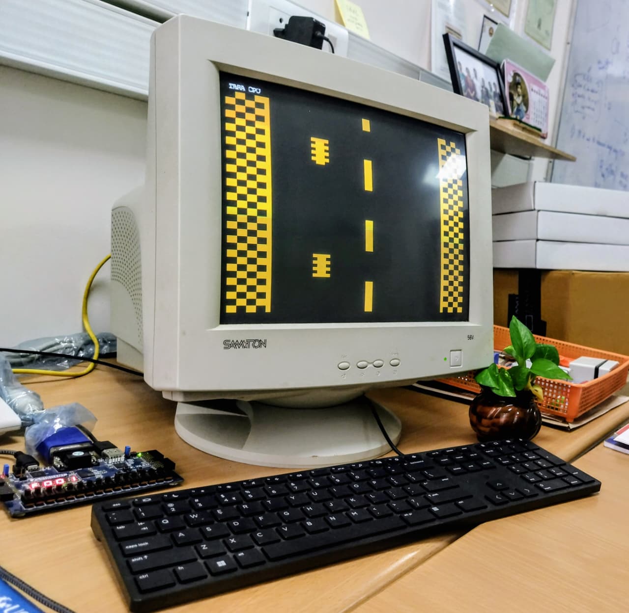
Try a game
- Use TARA Studio to Load & Run one of the games under
python-sim/tara_simulator_fpga/src/examples/progs/Games. - Set
sw[0]=1andsw[1]=1for fast auto-run. - Use the directional buttons or a USB keyboard. Use
sw[4]as the game quit bit if the program checks it. - Use TARA Studio's memory view at
0x600for512bytes only when you want to inspect the framebuffer bytes directly.
8. Troubleshooting
Most failures fall into one of three categories: the board was not configured with the expected bitstream, the CPU is being held or paused, or TARA Studio is connected to the wrong serial device. Work from the outside in: confirm power and programming first, then check switches and LEDs, then check the TARA Studio connection.
Running and connecting
| Symptom | Most likely cause | What to do |
|---|---|---|
| No VGA image | Board not configured, wrong monitor/cable, or still in reset/splash | Check DONE first. If it is off, program SRAM or boot flash with JP1 at QSPI. If it is on, check VGA and press BTNC. |
| Screen has banner but no program output | CPU not running or program draws nothing | Set sw[0]=1, check led[14] is off, check PC on seven-seg. |
| Seven-seg display is not the value you expect | Wrong display source or register select | Set sw[15:14] correctly; for registers set sw[13:11]. |
| FPGA USB radio button is disabled | pyserial is unavailable in the Python environment running TARA Studio | Run python -m pip install pyserial in that environment, restart TARA Studio, and reopen Connect Memory. |
| TARA Studio says no response | DONE is off, the wrong Digilent endpoint is selected, or the running bitstream does not include the current UART monitor | Confirm DONE, choose Connect Memory → FPGA USB, Rescan, and try the other Digilent endpoint. Reprogram the current tara_top.bit if needed. |
| Detect works but memory cannot connect | JTAG detection and the UART memory monitor are separate channels | A successful Detect proves the cable and JTAG chain, not the running TARA UART. Confirm DONE, the current bitstream, and the UART endpoint, then Connect. |
| Connect drops while FPGA programming starts | Normal hand-off while JTAG resets the fabric and TARA Studio temporarily closes UART | Wait for programming to finish. After SRAM programming the tool rescans and attempts reconnection; otherwise reopen Connect Memory. |
| Manual memory pokes disappear | Running program overwrote the same address | Pause with sw[0]=0 before writing, or use TARA Studio's load flow so the CPU is held during program transfer. |
Load & Run did not move the memory view to 0x000 | Expected behavior | The viewer Start address is intentionally preserved. Enter 0x000 and press Read only when you want to inspect the loaded instructions. |
| CPU looks stuck after enabling loader | sw[2]=1 with no valid JA loader driving active/sclk/sdata | Set sw[2]=0 for normal use. |
| Halted LED is on | The program executed HLT | Read the final registers, then press btnC or use Load & Run for another program. |
Programming the bitstream
| Symptom | Most likely cause | What to do |
|---|---|---|
| Setup dialog says openFPGALoader is required | The programmer is not installed, or is not on the PATH the application inherited | Install it (brew install openfpgaloader on macOS), or press Locate… and select the binary if you built it yourself. |
unable to open ftdi device: -3 (device not found) | Board not connected, not powered, or the cable is charge-only | Check the power switch and the power-good LED, reseat the micro-USB cable at callout 13, and try Detect before programming again. |
| Programming fails with a device or claim error | Another program holds the JTAG channel | Close the Vivado hardware manager or any other programmer, then retry. TARA Studio releases its own UART connection automatically while it programs. |
| Warning that the bitstream is for the wrong device | The .bit was built for a different FPGA | The Basys 3 is xc7a35tcpg236. Rebuild for that part, or pick the correct file — the grey line under the path shows which device each bitstream targets. |
| File is rejected as not a bitstream | Wrong file chosen, or a truncated or corrupted download | Choose the .bit written by the build, normally verilog/CPU/build/tara_top.bit, and re-copy it if the size looks wrong. |
| Design disappears after switching the board off | It was loaded into FPGA SRAM, which is volatile | Expected. Program again after each cold boot, or use SPI flash so the board reloads the design by itself. |
| SPI flash reports success, but PROG or power-cycle leaves DONE off | JP1 is still in JTAG mode, so the FPGA is not trying to boot QSPI flash | Turn power off, move JP1 at callout 10 to QSPI, turn power on, and check DONE. Reflash only if QSPI mode still fails. |
| Pressing the red PROG button makes the design disappear | PROG cleared the SRAM image, then the source selected by JP1 did not provide a valid configuration | Put JP1 at QSPI if a flash image is installed, or use Board Setup to program SRAM again. |
Pressing BTNC does not reload flash | BTNC resets only the TARA CPU | Use the red PROG button at callout 9 or power-cycle to restart FPGA configuration. |
9. Quick Reference
Keep this section nearby once the basic workflow is familiar. It collects the memory map and the board pins that matter to the top-level module.
Configuration, boot, and reset
| Action | Result | What remains |
|---|---|---|
| Board Setup → FPGA SRAM | Configures and starts TARA immediately over JTAG | Cleared by PROG or power-off |
| Board Setup → SPI flash | Stores a persistent configuration image | Survives power-off; boot it with JP1 at QSPI |
| Red PROG button | Restarts FPGA configuration from the source selected by JP1 | Clears the current SRAM configuration first |
| Power cycle | Restarts the board and FPGA configuration | SRAM is lost; QSPI flash remains |
| Center BTNC | Resets the running TARA CPU and starts at PC=0x000 | FPGA configuration and flash are unchanged |
| Load & Run | Assembles and writes a .tara program at 0x000 | The memory viewer Start address is unchanged |
Memory map
| Address range | Size | Meaning |
|---|---|---|
0x000-0x5FE | 1535 bytes | Program, data, stack, and ordinary memory. |
0x5FF | 1 byte | Live input port for buttons/keyboard/quit. |
0x600-0x7FF | 512 bytes | Framebuffer read continuously by VGA hardware. |
Basys 3 pins used by top-level ports
| Signal | Pin | Signal | Pin |
|---|---|---|---|
clk | W5 | btnC | U18 |
btnU | T18 | btnD | U17 |
btnL | W19 | btnR | T17 |
RsRx | B18 | RsTx | A18 |
PS2Clk | C17 | PS2Data | B17 |
JA[0] | J1 | JA[1] | L2 |
JA[2] | J2 | Hsync/Vsync | P19/R19 |
Appendix A. Source Code Guide
This appendix is the merged source-code guide. Read it when you want to move from operating the board to understanding how the Verilog and simulation model fit together. The main manual explains what the running system does; this appendix explains where that behavior lives in the repository and how to rebuild it with confidence.
A.1 Repository at a glance
The verilog/CPU tree is deliberately split by responsibility.
The hardware directory contains everything that becomes
logic on the FPGA. The tools directory contains support
utilities used by the build and verification flow. User-facing program
loading and live memory inspection are handled through TARA Studio, so
the hardware source tour stays focused on the synthesizable design and
the build resources that support it.
hardware/
the chipStart here when you want to understand what Vivado synthesizes. The top-level board wrapper, CPU datapath, control unit, memory, VGA, UART, and testbenches all live under this directory.
tools/
the build support filesThese files support the hardware build and verification flow. They are implementation resources, not the normal entry point for using the board in a lab session.
manual/tarahw/
the reference material
Use this manual for lab operation and REQUIREMENTS.md
for exact ISA and microarchitecture details. Shared figures are
stored under manual/figs.
A.2 How to study the source
Read the design top-down. Begin with the board wrapper so you know which external signals exist, descend into the CPU integration file, then open the control unit and the leaf datapath blocks. Keep one organizing idea in view: TARA is microprogrammed. The behavior of each instruction is not scattered through ad hoc control logic; it is encoded in a generated control ROM that is indexed by opcode and T-state.
- Start with the contract. Skim
REQUIREMENTS.mdfor the ISA, memory map, instruction formats, and 40-bit control word layout. - Open the board top level.
hardware/rtl/board/tara_top.vconnects the CPU to clocking, reset, VGA, buttons, keyboard input, UART, seven-segment display, and LEDs. - Read the processor shell.
hardware/rtl/cpu/tara_cpu.vshows how the register file, PC, IR, MAR, MDR, ALU, memory, and control unit exchange data. - Follow the control path.
hardware/rtl/control/contains the T-state ring counter, ROM lookup, and decoded control signals that steer the datapath. - Compare RTL with the control-store support files. The micro-operations for each instruction are kept in the build support area.
- Finish with the leaves. The reusable pieces in
rtl/core/,rtl/alu/, andrtl/mem/are small enough to read after the system shape is clear.
tools/microcode/microcode_listing.txt. It prints each
opcode and T-state with the asserted control signals, which is the
fastest textual view of what the CPU will do cycle by cycle.
A.3 Module hierarchy
The tree below is the useful mental map for reading the Verilog. It is not just a file list; it shows where board-level concerns stop and where the processor proper begins.
A.4 Build and data flow
A TARA bitstream is not produced from Verilog alone. Before Vivado
builds the design, the support tooling prepares the memory images that
the hardware expects for control and boot-time initialization. Vivado
then combines those files with the RTL and constraints to produce
build/tara_top.bit. After the board is configured, TARA
Studio can replace the program in live memory over USB without changing
the FPGA configuration.
build.tcl
combines them with the Verilog and constraints; the saved bitstream
configures the board; and TARA Studio talks to the running system
over USB.
A.5 Building the bitstream
Prerequisites
| Need | Used for |
|---|---|
| Xilinx Vivado, 2022.2 tested | Synthesis, implementation, and bitstream generation. Needed to build a bitstream, not to load one. |
| Python 3 | Build support scripts and co-simulation. |
| TARA Studio desktop application | Programming a prebuilt bitstream over JTAG, program loading, live memory inspection, and FPGA interaction. |
| openFPGALoader | Used by TARA Studio to configure the board. Only required on machines that program hardware without Vivado. |
| Icarus Verilog | Optional, for the RTL testbenches in hardware/sim. |
One-command flow
Call Vivado from the CPU/ root after the repository has
been prepared. With the board attached, the default flow builds and
programs; with noprogram, it only writes the bitstream and
reports.
vivado -mode batch -source hardware/build.tcl
vivado -mode batch -source hardware/build.tcl -tclargs noprogram
build.tcl reads hardware/rtl/**/*.v and
hardware/constraints/tara_basys3.xdc, supplies the required
memory initialization resources, and writes outputs under
build/. If you use the Vivado GUI instead, create a project
for xc7a35tcpg236-1, set tara_top as the top
module, and add the XDC file.
build/tara_top.bit is the only artifact needed to bring up a board.
Distribute that one file and every other machine can program hardware from
TARA Studio without a Vivado installation — see
section 3.
A.6 Simulation and verification
The design is checked at two levels. The Python co-simulation compares the microcoded hardware model against the reference simulator, while the RTL benches exercise the actual Verilog blocks where Icarus Verilog is available.
Cycle-accurate co-simulation
python3 tools/model/verify.py
This command lock-steps tools/model/tara_pymodel.py against
the golden simulator in ../python-sim. Both decode the same
instruction behavior, and the hardware model reads the same prepared
control words used by the RTL, so mismatches expose real drift in the
microcode or datapath assumptions.
RTL testbenches
cd hardware/sim
make
make cpu
make clean
Use the simulation Makefile for local HDL-level confidence before opening Vivado or when changing shared datapath modules.